Humanity already knows how to turn light into electricity and how to create batteries without chemical reactions, but these devices have very low efficiency. Nanomaterials based on two-dimensional structures show the most promising characteristics, however they are very difficult to obtain, and scientists struggle to control their properties.
If it was possible to controllably narrow the bandgap, one of the key parameters concerning nanomaterials and something which determines the nature and magnitude of a substance’s conductivity, it would radically change the fields of nanoscale semiconductor electronics, optoelectronics, and spintronics. With this development, materials with the exact properties necessary for this device could be created on an industrial scale. Today, these materials are made from “what is accessible”. The possibility of controlled variation of the optical, electronic, and magnetic properties in two-dimensional materials was predicted quite a long time ago. But yet, despite great efforts, scientists could not experimentally prove this theoretical prediction until a group of scientists led by Professor Dmitri Golberg tackled the problem.
“For the first time in the world, a group of scientists from NUST MISIS (Moscow, Russia), the National Institute for Materials Science (NIMS, Japan), Beijing Jiaotong University (P.R. China), and Queensland University of Technology (Australia), and led by Professor Dmitri Golberg, one of the world’s leading scientists, has managed to solve the problem of two-dimensional materials with controlled properties”, said Alevtina Chernikova, Rector of NUST MISIS.
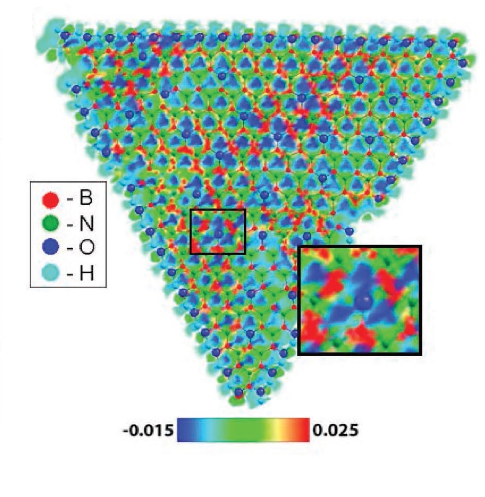
In an article published in the journal Advanced Materials, scientists describe the world’s first experiment on the controlled creation of material based on partially oxidized boron nitride. The material is made through the gradual addition of oxygen into the structure of two-dimensional boron nitride. Scientists managed to narrow the bandgap only by introducing carbon atoms into boron nitride, but this method has proven to be both very difficult and very expensive. The partial oxidation method is much simpler and cheaper.
After synthesis, scientists measured the width of the bandgap of partially oxidized boron nitride by depending on the content of lattice of oxygen atoms. During the experiments on prototypes it was possible to prove the theoretically predicted properties of boron nitride’s crystal lattice for several levels of the oxygen content.
“The key achievement of our work is that we have managed to successfully combine methods of theoretical materials science with the magnificent work of our fellow experimenters. On the one hand, our close cooperation has resulted in the fact that we have managed to successfully synthesize new material based on boron nitride with the possibility of controlling the width of the bandgap; and on the other hand, features of its properties have been thoroughly investigated on a theoretical level; with this experimental data we successfully proved the theory”, said co-authors of the work, assistant professors at the NUST MISIS Laboratory of Inorganic Nanomaterials, Pavel Sorokin, Dr. of Physical and Mathematical Sciences, and Dmitry Kvashin, Candidate of Physical and Mathematical Sciences.
With the help of comprehensive studies of the obtained material, scientists were able to understand how and why the width of the bandgap in partially oxidized boron nitride changes:
“The presence of hydroxyl groups, located on the edges of the new materials, makes the main contribution to the narrowing of the bandgap. The presence of such a layer leads to the formation of additional electronic levels near the Fermi energy, which leads to a narrower width of the bandgap, observed experimentally”, — noted Sorokin.
The scientists noted that this method of narrowing the bandgap may lead to active use of this material in such fields of science and technology as photovoltaics, optoelectronics, and energy storage.
The resources of the NUST MISIS Cherry supercomputer cluster were used in the theoretical part of the work. The practical part was carried out in Japan and Australia.
The work was conducted through the “Theoretical materials science of nanostructures” infrastructure project created by NUST MISIS as part of the Competitiveness Enhancement Program of Leading Russian Universities among Global Research and Education Centers (Project