An international team of scientists led by NUST MISIS and TU Dresden Professor Gotthard Seifert, one of the leading specialists in the field of two-dimensional materials, has solved a problem that has for almost half a century prevented the use of two-dimensional materials in microelectronics. The paper was published in ASC Nano journal.
For over 40 years, two-dimensional materials have been positioned as the future basis of microchips, and in general as the basis for next-level microelectronics. Scientists’ optimism is easy to understand — these are the thinnest semiconductors possible, and they will provide an unprecedented miniaturization of devices. This is particularly important for compounds such as monolayer molybdenum disulfide, which consists of a metallic molybdenum plane located between two layers of sulfur. A perfectly made monolayer molybdenum disulfide is an excellent semiconductor with not only electronic, but also optical features.
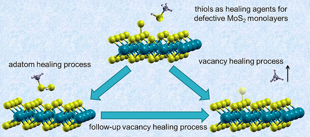
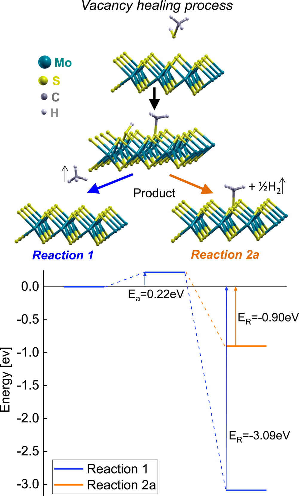
While physicists have repeatedly been trying to prove the suitability of this compound for micro- and nanoelectronics, chemists have been struggling to achieve the most efficient way to obtain it. They invented many ways but even when using the most effective ones, the layers they obtained had many defects. This is the shortcoming in the structure of a two-dimensional layer of atoms of sulphur or molybdenum, and vice versa (an excess) for sulfur atoms. Each defect affects the semiconductor’s properties, and even makes its industrial application impossible, because no one could manage to create two samples of molybdenum disulfide with identical parameters. That is why scientists faced the problem of creating the perfect monolayer. Scientists have now managed to solve this by discovering that there is a mechanism for a full recovery of defects in monolayers of molybdenum disulfide, one of the most promising materials used for nanoelectronics
“The creation of two-dimensional materials is one of the most promising areas of modern materials science. The breakthrough work of the international team of scientists from Germany and the USA led by Professor Gotthard Seifert, one of leading specialists in the field of two-dimensional materials and a professor at NUST MISIS and TU Dresden, opens up great opportunities for two-dimensional materials in modern microelectronics”, said Alevtina Chernikova, Rector of NUST MISIS.
As explained by Professor Seifert, the science team has managed to solve not one but two problems, since the difficulty in creating reproducible samples of molybdenum disulfide is not only due to monolayers have defects. Even the perfect monolayer degrades over time, especially when exposed to air. This makes the research even more relevant.
“In our work, for the first time, we have demonstrated a mechanism to fix structural defects in existing samples of monolayer molybdenum disulfide. Moreover, our calculations, supported by our experiment, helped us to not only understand that this mechanism does exist, but also allowed us to figure out how it needs to go. Our research results really open up a whole field of possibilities for the practical use of molybdenum disulfide monolayers and related compounds as key elements of various circuits. Surely, the discovery of such a mechanism doesn’t mean that we can create an infinite monolayer, or, for example, a monolayer with the length of a kilometer. More than likely, we are talking about structures of micrometer size. However, with account of trends toward the miniaturization of electronics, we don’t need huge monolayers”, commented Professor Gotthard Seifert.
According to Professor Seifert, the next step in his work, which he is planning to do with the NUST MISIS science team, is the study of other two-dimensional materials and their potential opportunities and application in electronics.