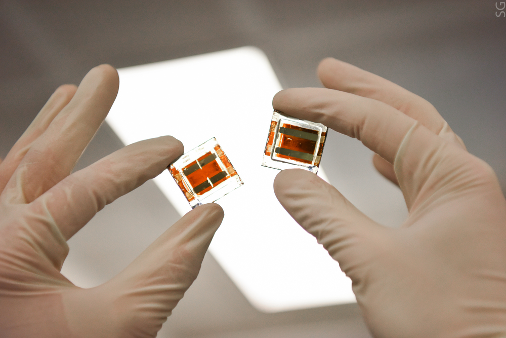
Scientists from NUST MISIS and IPCE RAS (Moscow, Russia) together with Italian colleagues from University of Rome Tor Vergata managed to significantly increase stability and effectiveness of perovskite elements — promising materials for solar energy — by adding a layer of copper iodide (CuI). The article on the research is published in “Materials”.
Hybrid perovskite materials is a young class of semiconductors for optoelectronics, which is considered an effective and affordable alternative to silicon in the production of solar cells. Hybrid perovskite materials are much cheaper, as they can be printed by liquid application methods at low temperatures (<200 C).
Team of scientists form the National University of Science and Technology “MISIS” and Frumkin Institute of Physical chemistry and Electrochemistry of Russian Academy of Sciences under the guidance of Professor Aldo Di Carlo (University of Rome Tor Vergata) decided to eliminate the main imperfection, which prevents this “alternative” from being widely produced — instability. The key role was played by the molecule of methylammonium lead iodine (MAPbI3).
“MAPbI3 photoactive layer crystallizes on the surface of a p-type transport layer carrying positive charges (NiO in our case). As we know, under constant illumination and subsequent heating of perovskite solar cells with a photoactive layer of MAPbI3, free iodine and hydrogen acid are released, which harms the interface between the layers of perovskite and NiO, forming a set of defects and significantly reducing the stability and performance of the device”, Danila Saranin, researcher at NUST MISIS Laboratory for Advanced Solar Energy“, explains.
To solve this problem, scientists used an additional layer of p-type copper iodide semiconductor between perovskite and hole transport NiO layer.
“This material does not demonstrate such rapid degradation, accompanied by the release of iodine compounds similar to the used perovskite material, when exposed to light. Moreover, the additional p-layer allowed to improve the collection of positive charges and significantly reduce the concentration of defects in the transition between the photo-absorbing and hole-transport layers”, Danila Saranin adds.
Stabilizing the perovskite element of a similar architecture and composition of the photoactive layer by adding organic layer is not a completely new idea. But other teams used expensive and complex (in terms of synthesis) materials: derivatives of organometallic compounds of ferrocene and low molecular weight organic semiconductors.
Now, scientists for the first time tried using CuI (copper iodide) — a more accessible and easy-to-use inorganic material. This hypothesis was proved by the results of the experiment: the improvement of the structure of the perovskite element increased the stability of its work by an average of 40%, and the efficiency increased to 15.2%.
According to the scientists, the thickness of the final element is less than 1 micron — ten times less than that of silicon solar panels.
Further, scientists plan to create a similar layer to stabilize the transmission of negative charges, as well as to scale the technology to the size of a large-format module.
