For the first time ever, the representative of a family of 2D substances — copper oxide — was experimentally obtained. The substance has already demonstrated some unusual properties which can not only expand the field of experiments with graphene, but also can set a new direction in microelectronics. An article on the achievement of the scientists from NUST MISIS, FSBI TISNCM, IBCP RAS, and international colleagues from NIMS (Japan) was published in the prestigious journal NanoScale.
An international team of physicists predicted and experimentally proved the existence of a new family of inorganic compounds. Pavel Sorokin, Doctor of Physical and Mathematical Sciences, senior research fellow at the NUST MISIS Inorganic Nanomaterials Laboratory, and head of the “Theoretical Materials Science Nanostructure” infrastructure projects, stated that this is a case of the world`s very first two-dimensional material with square crystal lattice, or in other words — copper oxide.
The creation of one-atom-thick 2D materials is a promising area in materials science today. Since the discovery of graphene in 2004 as the first 2D material, researchers across the world have been hard at work studying its properties, and trying to combine it with other materials.
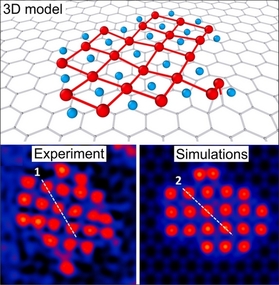
By studying different properties of graphene, researchers conducted the synthesis of a new family of substances. That’s why the island regions of 2D copper oxide are located on a graphene base. According to Dr. Sorokin, “the synthesis on a graphene core is currently the only opportunity to get these 2D materials. However, with the development of technologies this limitation can be overcome”.
Unlike graphene with its hexagonal unit cells consisting of carbon atoms, 2D copper oxide has a square lattice. “Up until now, scientists were able to synthesize the materials with hexagonal lattice, for example, various derivatives of graphene or boron nitride. Flat square metal grating is unstable, however, but the compound of copper with oxygen stabilized it”, said Pavel Sorokin, senior research fellow at the NUST MISIS Inorganic Nanomaterials Laboratory.
The method the scientists used opens a wide range of opportunities for the synthesis of a new family of materials. In fact, scientists were able to achieve the “self-assembly” of 2D copper oxide on graphene. To create a new substance, the scientists from the National Institute for Materials Science (Japan) settled copper atoms from the gas phase to a partially oxidized bit of graphene. Then, the system`s heating led to the oxygen and copper atoms regrouping in to a new structure.
All the features of the new material have to be studied further for some time, however, there is something to say about the properties of 2D copper oxide. One of these unusual properties, predicted by Russian physicists Pavel Sorokin and Dmitry, was the antiferromagnetism (low magnetism) which usual copper oxide doesn’t show under any circumstances.
Researchers believe that there could be other applications for their work. According to Sorokin, “Our discovery proved that graphene can be used as a basic element for producing various materials, including not only standalone materials, but also multi-layer 2D heterostructures. In the presented experiment, a new monolayer structure with a set of unique properties which we have yet to study, was formed in grapheme”.
Antiferromagnetics have great potential in microelectronics. For instance, in order to write one bit of data on an antiferromagnetic material, only 12 atoms of its surface are needed, whereas current technology uses hundreds of thousands of atoms to write the same amount of data.
“NUST MISIS is a scientific-research and education center, which is one of the leaders in the field of materials science both in Russia and in the world. In 2017, NUST MISIS entered the QS World University Rankings by Subject for Materials Science with the highest score in the ‘Academic Reputation’ indicator, so the university is included in the top 30% of the best universities in this field. Our results became visible on a global level due to attraction of world-leading scientists, the launching of world-class laboratories, and the implementation of large-scale projects of a MegaScience level”, said Alevtina Chernikova, Rector of NUST MISIS.


