In Russia, a super-fast integrated optical detector has been presented that can be adapted for various tasks — from telecommunications and thermal imagers to medical biosensors, security systems, and astronomical instruments. The device detects weak infrared signals in an integrated-optical chip 100 million times faster than its analogues and updates data more than one billion times per second, making it one of the fastest in its class.
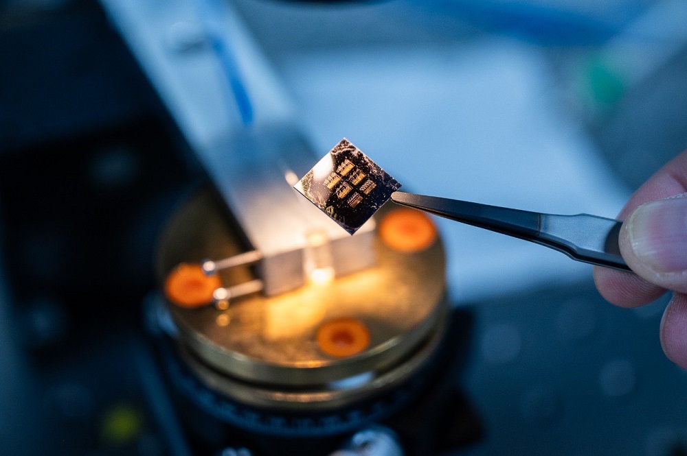
Photonic integrated circuits are microchips where one of the key tasks is converting optical radiation into electrical signals. Therefore, creating affordable, fast, and accurate detectors is a priority. To address this challenge, researchers from NUST MISIS, in collaboration with colleagues from HSE University, Skoltech, and MSPU, have developed an integrated-optical thermal receiver — a bolometer — based on films made of carbon nanotubes.
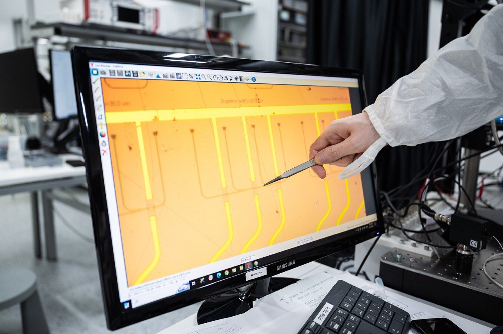
“The frequency range of the bolometer indicates how quickly the film heats up due to the absorption of infrared radiation. Our new detector operates at a frequency of 1 GHz, which exceeds similar devices based on nanotubes by almost 100 million times and can provide high-speed data processing in silicon nitride photonic integrated circuits,” shared Vadim Kovalyuk, head of the Laboratory of Photonic Gas Sensors at NUST MISIS.
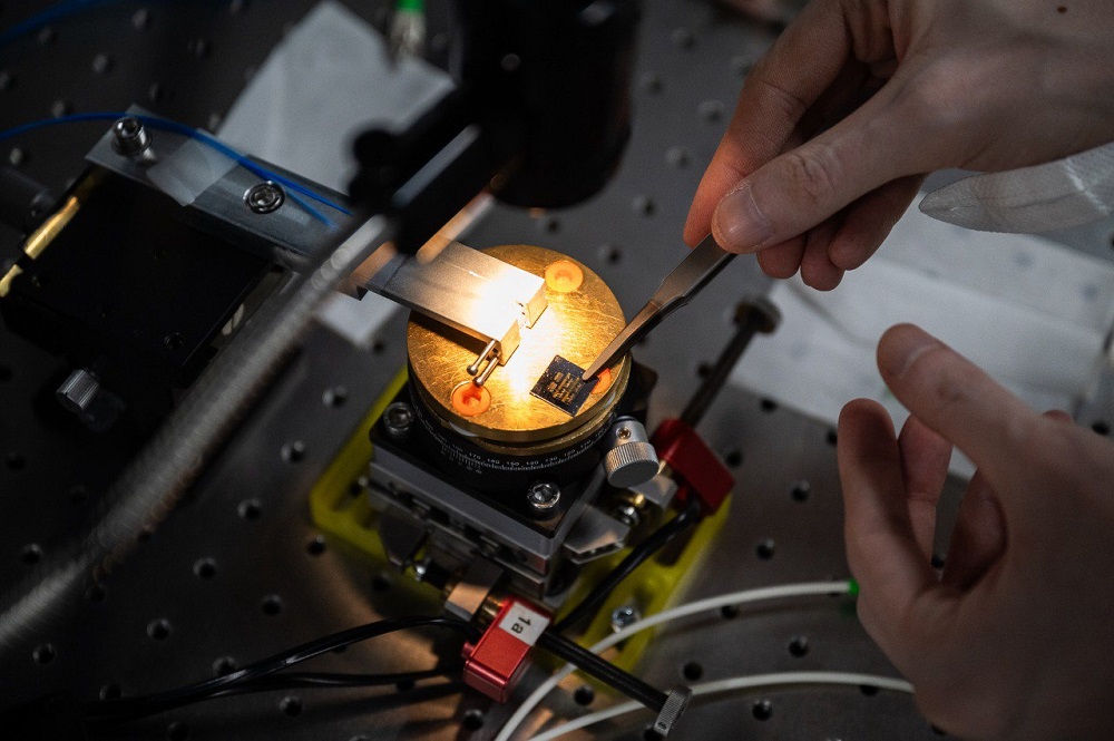
Modern bolometers are typically manufactured using complex multi-stage technologies such as chemical vapor deposition or crystal growth. Films made of single-walled carbon nanotubes significantly simplify production: they can be transferred onto surfaces without liquids or expensive chemicals through dry transfer methods, ensuring uniform and precise coverage. These films adhere well to virtually any material, including flexible and transparent substrates used in smartphones, portable sensors, or environmental monitoring equipment. By controlling the parameters of carbon nanotube growth, the composition of the coating can be modified. For example, to enhance electrical compatibility with the receiving circuitry or improve the absorption of electromagnetic waves of specific wavelengths.
“In our study, we relied on the well-known equation of thermal balance, which governs the operation of bolometers and shows that for the same material of the bolometer film, the ratio of sensitivity to the ultimate operating speed of the device remains constant. In other words, increasing the sensitivity of the detector inevitably leads to a proportional decrease in detection speed. Using inexpensive semiconductor amplifiers allowed us to compensate for the loss in sensitivity while significantly improving the response time of the photodetector. Moreover, the method of dry transferring the carbon film onto silicon nitride optical waveguides created conditions for highly efficient coupling, enabling nearly complete light absorption within a compact design,” explained Pavel An, a research associate at the Quantum Detectors Laboratory at MSPU.
The rapid response of the new bolometer is enabled by the unique properties of carbon nanotubes: their high electrical and thermal conductivity combined with low heat capacity. These results open promising prospects for the use of bolometers based on carbon nanotube films for quick data processing, fully optical neural networks, and coprocessors based on photonic integrated circuits in microelectronics or telecommunications. Detailed findings were published in Applied Physics Letters (Q1).
This work was supported by grants from the Russian Science Foundation (projects No.
and No.
and the Ministry of Science and Higher Education of the Russian Federation (No. FSME-2022-0008).