If scientists want to achieve stable and more qualitative results, they have to change the core of the scanning probe microscope — a piezoelectric plate. Additionally, the new material — biblast-furnace lithium niobate — allows scientists to study the surface at previously unattainable temperatures.
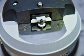
Scanning probe microscopes are research instruments that allow scientists to not only study objects at the nanoscale level but also to manipulate them with high precision. The principle of operating such microscopes is based on “probing” the sample surface with a cantilever — a miniature needle. Researchers have to move this needle very precisely, only a few nanometers. Actuators, special devices that operate on the basis of the piezoelectric effect, are used for this purpose. It can be seen in piezolighters where pressing a button causes a sharp deformation of quartz crystal and the appearance of an electric spark. The opposite effect works in scanning probe microscopes — the applied electric voltage deforms the crystal where the needle is attached. By changing the voltage, it is possible to move the needle line by line and scan the surface this way.
Today, tubes from lead zirconate titanate are used as a piezoelectric in the majority of scanning probe microscopes. These tubes have a lot of advantages over their counterpart, but they are not perfect either. For example, due to phenomenon like mechanical hysteresis, when scanning the cantilever might move to an unpredictable point, and the piezoelectric`s low resistance to temperature changes leads to the experiment’s results depending on the “weather” in the laboratory.
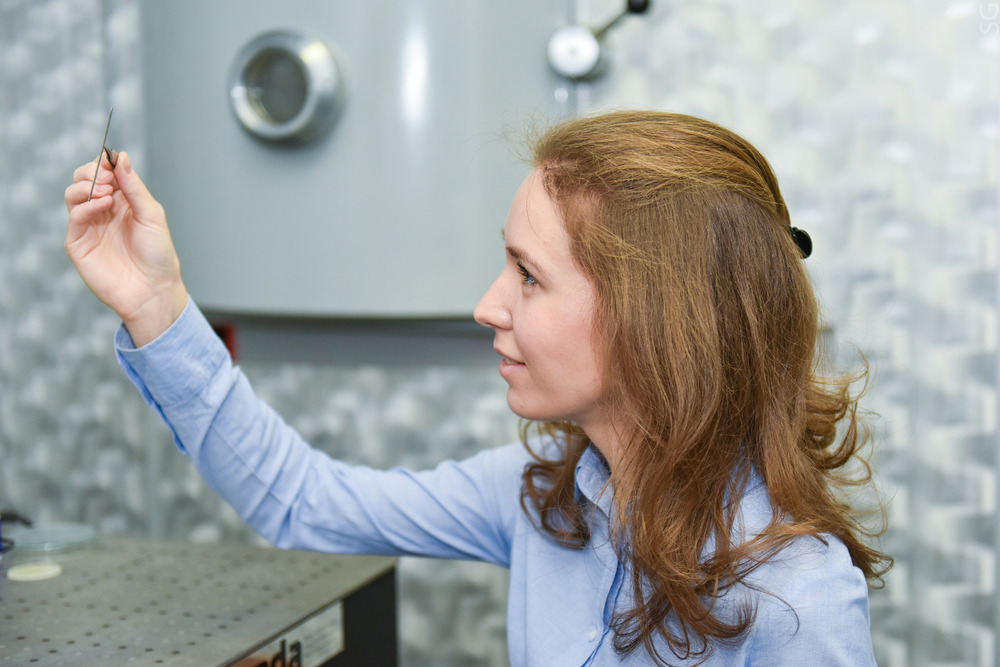
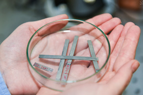
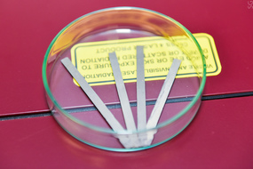
Yulia Terekhova, researcher at the NUST MISIS Department for Materials Science of Semiconductors and Dielectrics, has proposed replacing lead zirconate titanate ceramics with biblast-furnace monocrystals of lithium niobate, a new material developed at the Department for Materials Science of Semiconductors and Dielectrics for moving cantilevers.
Lithium niobate itself has been known for a long time — the first samples were obtained in the 1960s by scientists from the USSR and the United States, independently of each other, for use in lasers and other optical devices. In addition to excellent optical characteristics, lithium niobate exhibits piezoelectric properties, but doesn’t possess the same disadvantages that lead zirconate titanate possesses.
The lithium niobate piezoelectric characteristics are much worse than that of piezoelectric ceramics, which until recently didn’t allow the material to be used in scanning probe microscopes: intense pressure had to be applied to the niobate with the aim to move the cantilever needle a sufficient distance. NUST MISIS scientists have managed to solve this problem. A thin crystal plate of lithium niobate is put down so that two similar equal-volume areas (domains) are formed when an electrical field is applied.
Such crystals are described as biblast-furnace. By choosing the plate`s proper geometry and orientation, scientists have managed to obtain significant displacements of the cantilever at small control voltages.
Images have become clearer thanks to the application of crystals from biblast-furnace lithium niobate. In addition, it now has become possible to research surfaces at temperatures unattainable for lead zirconate titanate ceramics. Lead zirconate titanate ceases to be a piezoelectric at 150 — 200°С, but niobate keeps its properties up to 450°С, which allows scientists to study changes of scanned surfaces in the heating process.
Under the terms of the U.M.N.I.K. contest that Yulia Terekhova recently won with her project, she will work with this material for the next two years. Currently she is working on creating laboratory samples, and then she will study their deformation, resonance, and temperature characteristics. The research’s result will be a finished device that can replace obsolete displacement systems in scanning probe microscopes.
“A year ago I took part in the U.M.N.I.K. contest but wasn’t really confident in my abilities because at that time I had just started working on this project. This time I applied for the contest having gone a long way in my scientific work. My colleagues from the Department for Materials Science of Semiconductors and Dielectrics supported me from the very beginning of the contest to its end. Winning the contest helped me to believe in myself, and it was a great start for my scientific career”, — said Yulia.
