Russian scientists have identified the most promising material for manufacturing photonic chips that manipulate light directly on the chip itself. The technology could enable photonic memory, fully optical neuromorphic networks, and other devices for transmitting and processing information.
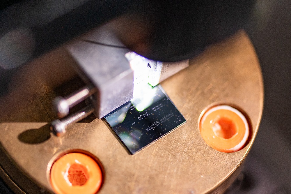
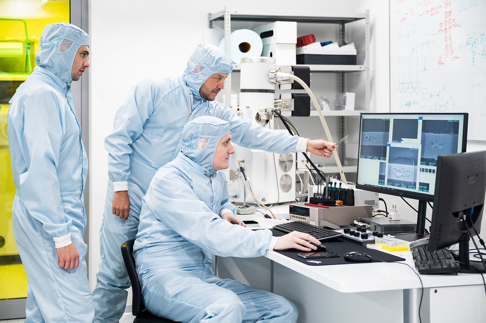
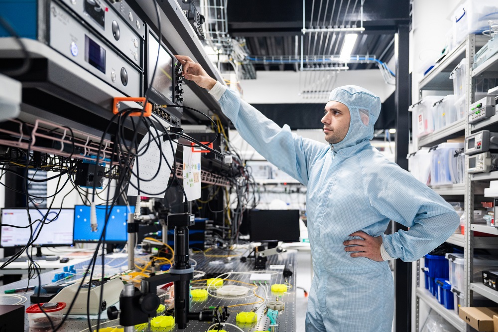
The potential applications of photonic chips are wide-ranging. They include optical processors for accelerating matrix multiplication—the core operation behind neural network training and inference; rapid disease diagnostics based on spectral light analysis; ultra-high-speed data transmission through optical fiber; compact solid-state LiDAR systems for autonomous vehicles; quantum key generation and distribution for secure quantum communications; and highly accurate optical sensors for industry, environmental monitoring, and agriculture.
“To control light on a chip, we studied phase-change materials that can switch their state under short laser pulses. Depending on the state, the material has either an ordered crystalline structure or a disordered amorphous structure, with dramatically different refractive indices. After laser exposure, the material retains its new state, making it suitable for information storage,” Grigory Goltsman, Doctor of Physical and Mathematical Sciences, Chief Research Fellow at the NTI Quantum Communications Competence Center at MISIS University.
Researchers from MISIS University, MIET, MPSU, Technological Center R&D Company, HSE University, and the Russian Quantum Center compared five compositions based on different germanium-antimony-tellurium semiconductor compounds and identified the most promising candidates. All materials were deposited onto identical silicon nitride waveguides—the structures that guide light through a chip. This approach made it possible to compare the intrinsic properties of the materials without changing the device design itself. The key factors were how strongly each material altered light transmission and how quickly it could switch between states. The detailed findings were published in the journal Materials Science in Semiconductor Processing (Q1).
“The results could change if waveguides made from other materials, such as silicon-on-insulator, or laser pulses with different wavelengths are used, so each material requires additional optimization. Our findings show that a material’s composition directly determines how well it performs for on-chip light control. At the same time, no single parameter is enough—you have to consider the signal modulation, switching speed, and the size of the material cell on a silicon nitride waveguide,” Alexey Prokhodtsov, Research Engineer at the Photonic Gas Sensors Laboratory at MISIS University.
The study could provide the foundation for developing photonic devices with non-volatile memory—systems that retain stored information without a continuous power supply.
“In the future, these technologies could be used in photonic computing and devices capable of storing and processing information with light. Before practical deployment, however, the selected materials must still be tested for durability, operational stability, and long-term state retention. This research is being carried out as part of MISIS University’s strategic technology project Quantum Internet under Russia’s Priority 2030 program,” Alexey Nevzorov, Candidate of Physical and Mathematical Sciences, Research Fellow at the NTI Quantum Communications Center at MISIS University, Priority 2030 postdoctoral researcher.
The research was supported by the Russian Science Foundation (Project No.
and the Russian Ministry of Science and Higher Education (Projects No. FSME-2025-0002 and No. FSMR-2024-0004).