A group of scientists led by Pyotr Lagov, Candidate of Technical Sciences and Associate Professor at the NUST MISIS Semiconductor Electronics and Semiconductor Physics Department, has developed a new type of power diode with an optimized silicon structure.
The application of these innovative diodes as part of manual or robotic welding machines increases the energy efficiency of the process and the quality of welded joints through a twofold increase of operating frequency up to 20 khz.
Robotic contact welding is widely used in machine engineering, shipping, the aircraft industry, and the production of household goods, and is the main method of joining multiple metal parts without the use of additives. Through this process, several dozen junctions can be created within a minute.
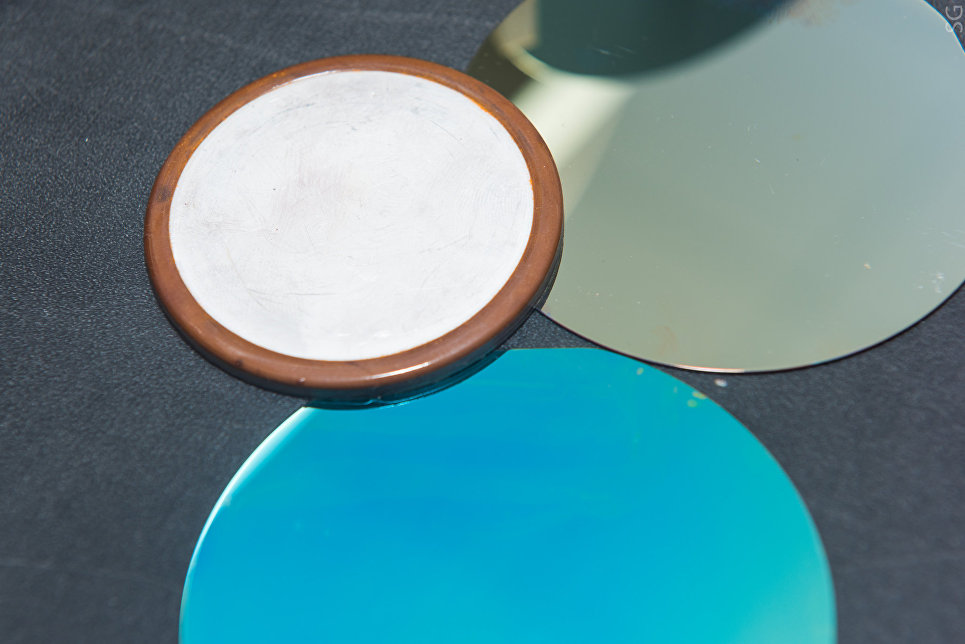
In the contact welding process, the impulse frequency of the current is the most important characteristic, as it directly determines the operation’s speed and performance, as well as the quality and durability of obtained welded joints. The NUST MISIS research team has developed a technology to obtain nanoscale recombination centers (atomic “vacancies”) in the structure of diode monocrystal. They are formed through a controlled atomic displacement (dislodging) from crystal lattice sites in certain layers of silicon plates of welding diode—the most important functional element of contact welding equipment.
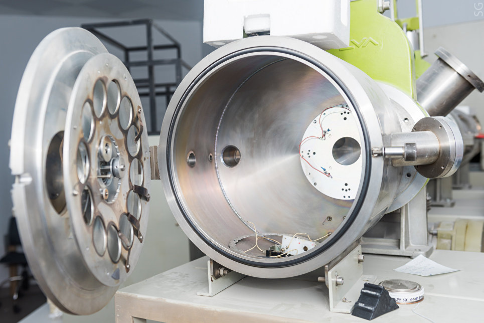
Atomic “vacancies”, or in simpler terms, micro-holes in layers of silicon structures, are obtained by applying a bombardment of finished monocrystal by light ions of high energy on an accelerator. As a result, structural defects at the atomic level of about 1 nm in size are formed in certain depths of thin
The technology of creating atomic “vacancies” allows scientists to increase the maximum operating frequency of diodes with a diameter of 50 mm from 10 to 20 kHz, while maintaining other characteristics. Today, the welding diode with this combination of characteristics vastly exceeds world analogues and can double the number of welding operations per unit of time, which means it allows for an increase in the speed of the mechanism assembly too.
Through this, the maximum operating frequency of the diode increases and the heating and cyclical changes of the temperature of the diode subsequently lead to wear and tear, which spurs mechanical damage and functional decrease. Under other equal conditions such a diode can provide a higher operating current of the welding and the accuracy of its restraints, as well as reduce the time period between individual working cycles, during which the diode`s cooling down (“rest”) takes place. This makes it possible to weld certain metals and alloys which cannot be welded at lower frequencies. In addition, such a diode is more resistant to different types of electrical overloads, which prevents the unit`s breakdown and holdup of the entire conveying assembly line. The increase in the operating frequency also reduces the size and weight of the transformer-rectifying unit of the welding machine, which is fixed on a robotic “hand” and works to reduce interference in an energy network, which facilitates an increase in the energy efficiency of automated production in general.
“We have not only developed a technology of the creation of recombination centers in the structure of power diode welding, but we also have obtained ready-to-use experimental samples of innovative diodes, which have competitive advantages — a maximum operating frequency no less than 20 khz (double the world’s best samples) at a current of 7 kA. Additionally, in a series of conducted work with a number of domestic enterprises, we have established that the technology of the local formation of recombination centers can be successfully applied in the production of silicon bipolar devices and integrated circuits of different classes. The large-scale introduction of this technology into semiconductor manufacturing will allow us to significantly improve the quality of the whole segment of the domestic electronic component base, which helps to ensure technological independence in terms of import substitution” — said Pyotr Lagov, head of the project.